您的瀏覽器不支援JavaScript功能, 若網頁功能無法正常使用時,請開啟瀏覽器JavaScript狀態 (Your browser does not support Javascript. For full functionality of this site, please enable JavaScript in your browser.)
ABOUT
PROGRAMS
Chinese Studies
Research
Natural Sciences
Engineering
Social Sciences
HIGHLIGHTS
FAQs
ABOUT
PROGRAMS
Chinese Studies
Research
Natural Sciences
Engineering
Social Sciences
HIGHLIGHTS
FAQs
SCROLL DOWN
News
Program Info
Program Info
Program Info
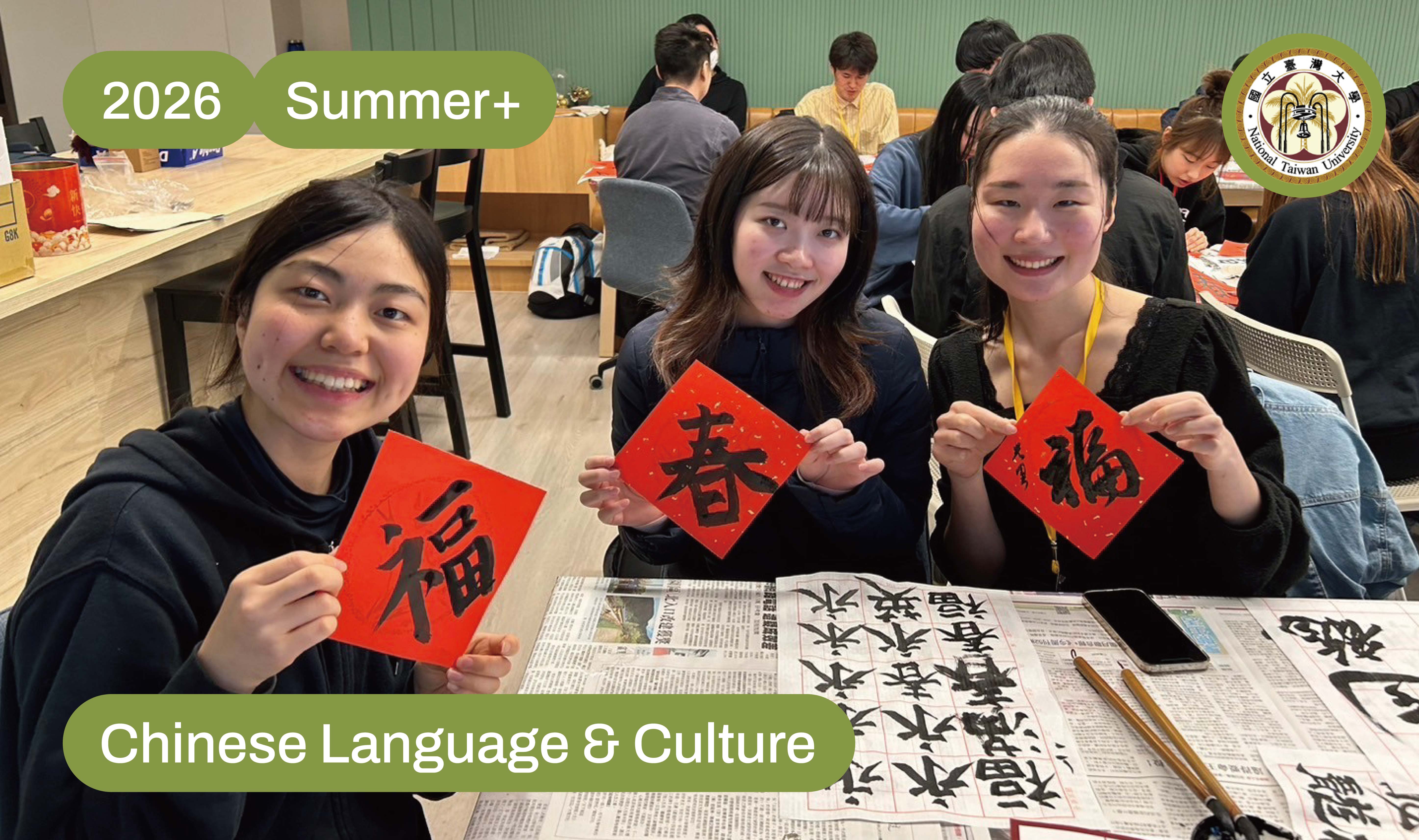
Summer+ Chinese Language & Culture
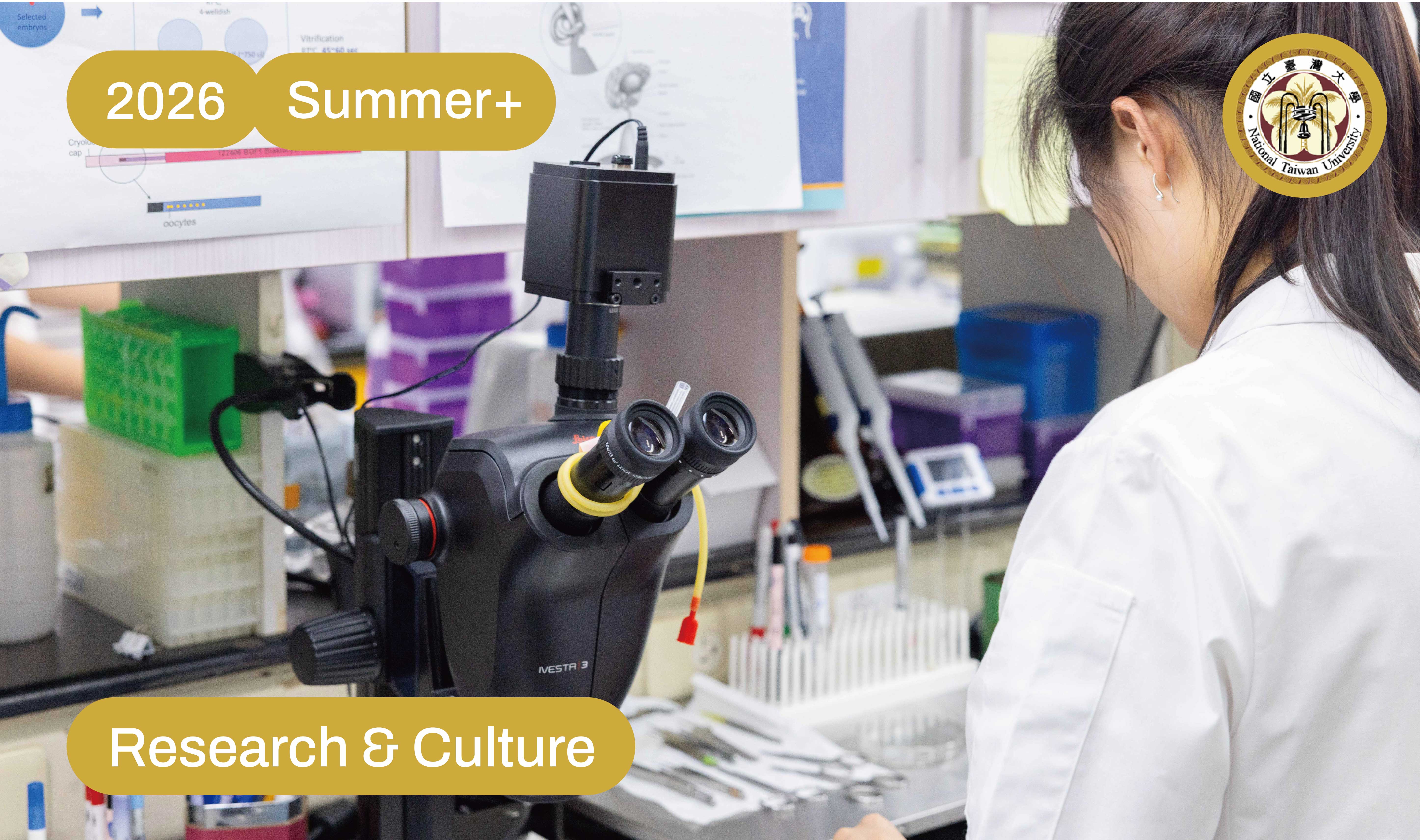
Summer+ Research & Culture
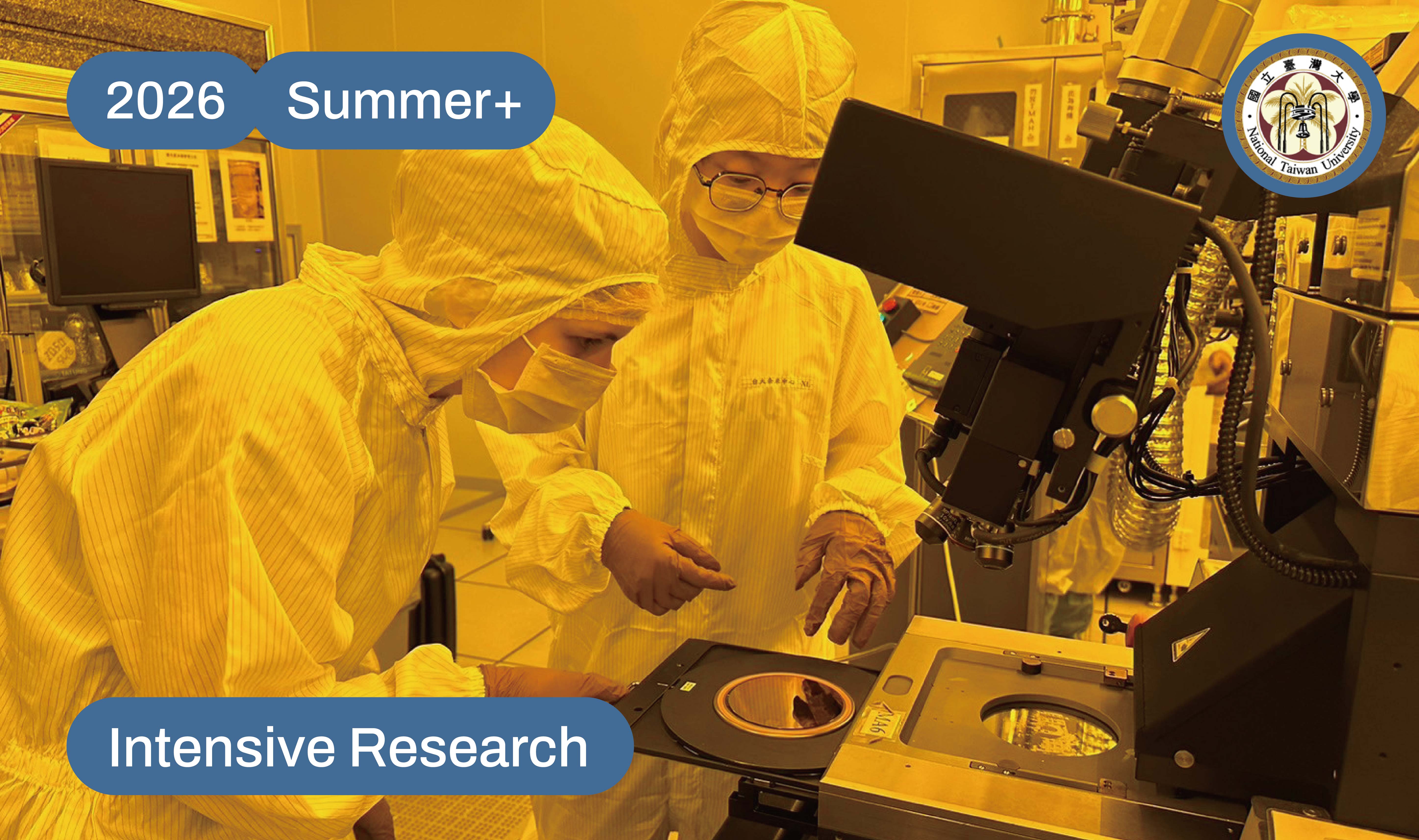
Summer+ Intensive Research
Program Info
Program Info
Program Info
Program Info
Program Info
Program Info
Program Info